The Lattice Writes the Law
The Lattice Writes the Law
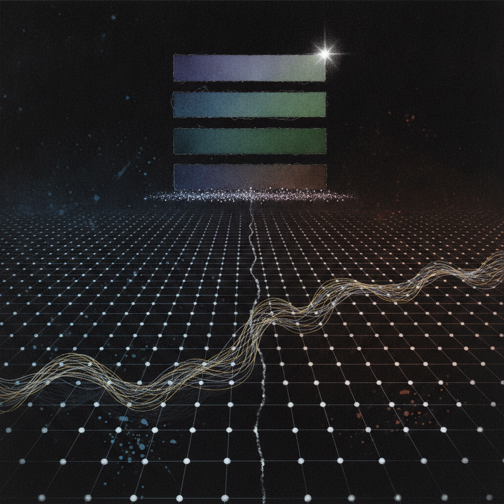
An electron in a crystal is never really free, and it is never really trapped either. It moves through a potential that repeats itself perfectly, atom after atom after atom, and Bloch's theorem says exactly what that repetition does to the electron's wavefunction: it can't destroy the periodicity, so the wavefunction becomes a plane wave multiplied by a function that shares the lattice's own period. The electron is neither a free particle nor a bound one — it is a traveling wave wearing the crystal's repeating pattern as a kind of uniform.
That constraint is what splits a continuous spectrum of possible energies into distinct allowed bands, separated by forbidden gaps where no wave of that period can propagate at all. Whether a material conducts, insulates, or does something interesting in between is decided almost entirely by where the last electron happens to land relative to those gaps — a full valence band and a large gap to the next available band makes an insulator; a small gap or an already-half-full band makes a metal or a semiconductor. The lattice doesn't just host the electron. It writes the law that says which energies are even available to be occupied.
Two different crystals, joined at a heterojunction, bring two different band structures face to face — and the electrons at that boundary inherit a compromise neither material offers on its own. Grade a layer of AlGaAs against GaAs and a thin sheet of electrons collects right at the interface, confined to two dimensions, freed from the donor atoms that would otherwise scatter them — a two-dimensional electron gas, existing only because two different laws met and had to be reconciled at a boundary a few atoms wide.
None of this is decided by intent. The Fermi-Dirac distribution simply says how likely each of those allowed states is to be occupied at a given temperature, and doping tips that occupancy toward donor or acceptor levels near the band edges. What looks like design — a semiconductor engineered for a purpose — is really just a very precise reading of a law the lattice was writing all along.