The runner leaves the rubble
The runner leaves the rubble
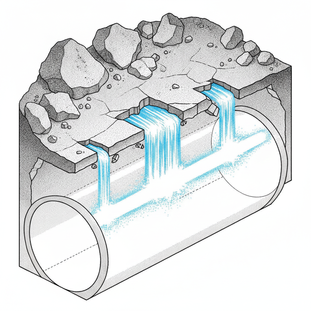
To make a semiconductor carry current, it must be doped. Atoms of a foreign element are violently violently embedded into the pristine silicon or gallium arsenide lattice, forcing them to donate free electrons to the material.
But this donation is a poisoned gift.
The very impurities that provide the electrons remain trapped in the lattice as ionized obstacles. When a voltage is applied and the electrons begin to sprint, they immediately crash into the jagged, charged rubble of their own donor atoms. This ionized impurity scattering creates drag, generating noise and capping the maximum speed of the transistor.
The High-Electron-Mobility Transistor (HEMT) solves the paradox by splitting the world in two.
It uses two different semiconductor materials sandwiched together. The first layer is heavily doped, choked with impurities that generously donate a massive cloud of free electrons. But because of a mismatch in the quantum bandgaps of the two materials, the electrons are energetically repelled by the rubble. They instantly spill over the border, falling into the adjacent, completely undoped, perfectly pristine layer.
Trapped in a two-dimensional quantum well in the clean layer, the electrons are spatially separated from the ionized donors that created them. The rubble remains on the upper floor, while the runners streak forward through an empty, frictionless corridor below, achieving sub-nanosecond switching speeds and ultra-low noise by leaving their origins behind.